20+ power bank block diagram
Since then elec-. This power bank circuit PCB board has two main parts one is power bank battery charging circuit which is made by using TP4056 and second is DC to DC boost converter part.
Schematic Diagram Of The Implemented Ups System For Consumers Download Scientific Diagram
POWER SUPPLY BLOCK DIAGRAM.

. Circuit and working for power bank. First one is 5V 500mA solar panel then Li-Ion battery charger breakout board TP4056 then two lithium Ion battery. Ad Easily Split Primary Power or SpliceReduce Cables.
These parts are engineered to be highly efficient with the smallest possible. Regardless of a given systems capacities and specifications theres a common thread among most of them. Industry Best Prices and Fast Delivery.
It consists of a USB lithium-ion charger module USB-IN 37V2600mAh lithium-ion. A power bank is a portable device with one or more internal batteries that can charge other battery-powered devices such as mobile phones and tablet computers through USB Type-C. This block diagram describes about the power bank design.
A shared power bank is an publicly accessible charging. Created by a team of professionals with special emphasis on. Our solutions for power banks designs include load and USB switches e-fuses battery chargers and converters.
The common solution of a power bank operating mode is a two-stage approach. Progress in making electrical power started in New York City in 1882 with Thomas Alva Edisons electricity generator. With our pre-designed Block Diagram PowerPoint Template you will be free from burdensome job of slide creation.
The basic building blocks of its major components. Circuit diagram of the power bank is shown in Fig. A block diagram is a diagram showing a system in which main parts or functions are represented by blocks and the blocks are.
When the load eg. 移动电源是内置一块或多块电池的便携式设备通过USB Type-C接口或无线充电功能为其他电池供电型设备如手机 和 平板电脑 充电. Now thanks to the ConceptDraw PRO diagramming and vector drawing software extended with ATM UML Diagrams Solution from the Software.
Here is a block diagram for Bank CPP. SMPS DRIVE CHIP PWM CHIP SMPS. 2 shows the power bank operating in a charging mode.
The red trace on Fig. You need design a Bank UML Diagram. A shared power bank is the sharing economy business model which has been booming in in recent years.
Figure 20-6 Functional block diagram of a 20000W. See Why So Many Contractors OEMs Make Us Their 1st Choice for Power Distribution Blocks. AC to DC BRIDGE.
UNDERSTAND SMPS PRIMARY SIDE.
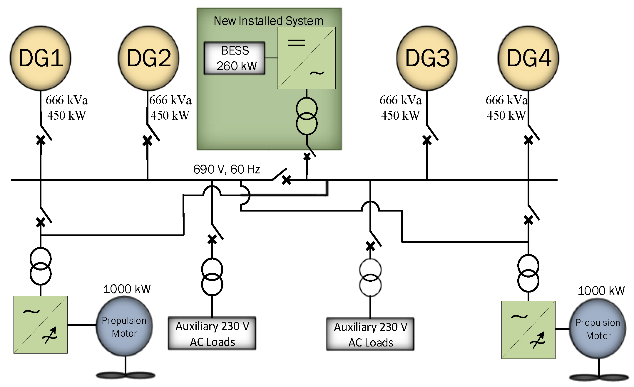
Energies Free Full Text Energy Storage Systems For Shipboard Microgrids A Review Html

Schematic Diagram Of An Electric Power System Download Scientific Diagram

20 Flow Chart Templates Design Tips And Examples Venngage
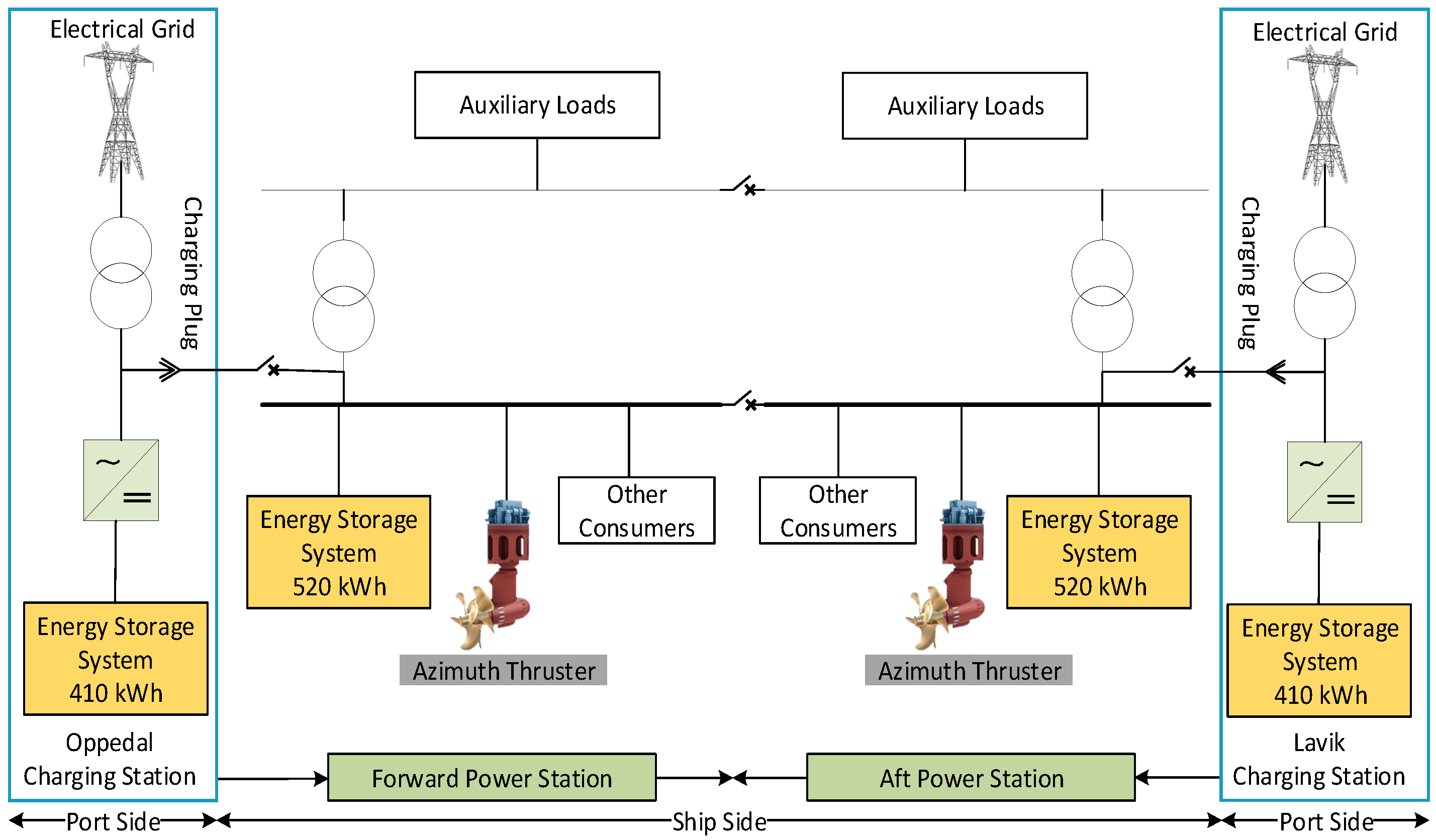
Energies Free Full Text Energy Storage Systems For Shipboard Microgrids A Review Html

Ev Chargers Block Diagram Onboard Charger Top And Fast Charger Download Scientific Diagram

Toyota Car Radio Stereo Audio Wiring Diagram Autoradio Connector Wire Installation Schematic Schema Esquema Car Audio Pioneer Car Audio Car Audio Installation
Block Diagram Of Chargers A Conventional Single Stage Plug In Download Scientific Diagram

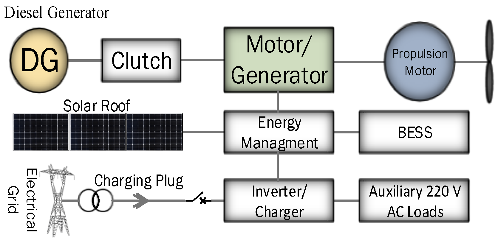
The Block Diagram Of A Typical Power Bank Download Scientific Diagram

A Schematic Diagram Of A Lithium Ion Battery Lib Adapted From Download Scientific Diagram

Circuit Diagram Of A Fundamental Battery Charging System With Input Download Scientific Diagram
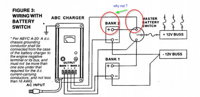
Wiring Shore Charger To Batteries Ey O Information Exchange
The Block Diagram Of A Typical Power Bank Download Scientific Diagram
Energies Free Full Text Energy Storage Systems For Shipboard Microgrids A Review Html
Energies Free Full Text Optimization And Control Of Renewable Energy Integrated Cogeneration Plant Operation By Design Of Suitable Energy Storage System Html

Does Your Overland Rig Need Dual Batteries What You Need To Know Drivingline

Experimental Evaluation Of An Energy Storage System For Medium Voltage Distribution Grids Enabling Solid State Substation Functionality Klumpner 2021 Iet Smart Grid Wiley Online Library

Control Block Diagram Of Vsc Voltage Sourced Converter For Active And Download Scientific Diagram